Home
>
News
>
Corporate news
Corporate news
Kw class 940nm band high power quasi continuous bar laser
Driven by the demand of pumped solid-state lasers and fiber lasers, semiconductor lasers have developed rapidly in material structure, epitaxial method, preparation technology and other aspects, and their performance level has made breakthrough progress.
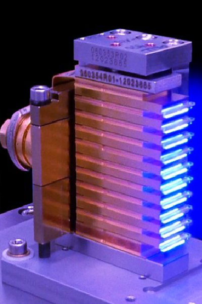
The high power semiconductor laser array (LDA) is generally applied in two ways: one is as a pump source, the high power bar pumps the crystal (Nd: YAG) to form a reliable semiconductor pumped solid state laser system; The other is to directly use the laser laser laser semiconductor, through the lens collimation, line array combined beam, stack array combined beam, the direct output power of semiconductor laser array can reach several kilowatts. The kilowatt-level 940nm high-power quasi-continuous bar laser studied by our company aims to increase the quasi-continuous output power of centimeter bar to over 1000W, changing the current situation of low power and brightness of bar.
In 2014, SPIE reported 88xnm KW class high power bar with dual active zone stacked epitaxial integration design, with a power output of 1.77kW at 0.28% duty cycle and temperature of 10 ° C. Double active area stacking epitaxy integrated design is to pile up two active areas vertically by one epitaxy growth, and the pn junction of two active areas is connected in series through Esaki tunnel junction. With this design, an electron can theoretically participate in optical recombination twice, so as to achieve the internal quantum efficiency close to 200% and twice the optical output, increase the slope efficiency of the laser, and effectively improve the optical output power density of the semiconductor laser. Figure 1 shows the structure and principle of stacked semiconductor laser with multiple active regions.
In order to fully realize the advantages of the above theory in practice, the design and manufacture of the laser must meet the following conditions: high photoelectric conversion efficiency of the single-layer laser, low resistance of the Esaki tunnel junction, inhibition of the chip transverse current expansion, high COMD threshold of the cavity surface, etc. Our company research and development technical team through the article to solve the structure and quality of epitaxial extension to the power limitation to improve the efficiency of single active area, the precise control of tunnel junction P and N heavily doped semiconductor growth to form a low resistance tunnel junction, development type deep ridge mesa etching process to achieve the transverse current suppression, break through the high power and the cavity surface treatment technology to improve the cavity surface damage threshold power, A series of important technical achievements have been made.


